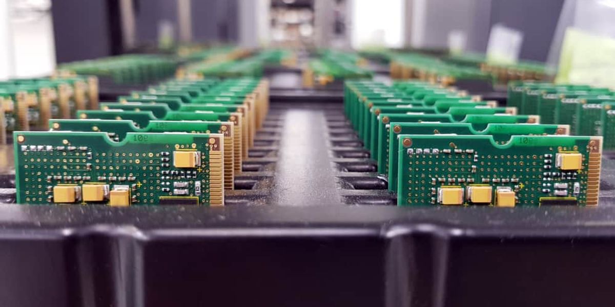
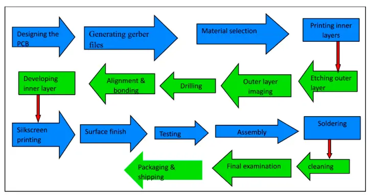
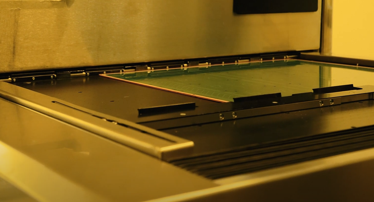
PCB Manufacture Process A Comprehensive Guide to Understanding and Circuit Diagram The PCB manufacturing process is a complex and multi-step journey that transforms a design concept into a functional electronic component. Each step, from design and material selection to final testing and inspection, plays a critical role in ensuring the production of high-quality, reliable, and efficient PCBs. In the PCB manufacturing process, etching is a process of removal of unwanted copper (Cu) from the board. The unwanted copper is nothing but non-circuit copper. As a result, the desired circuit pattern is achieved. Board manufacturers usually employ a wet etching process. In wet etching, the unwanted material gets dissolved when immersed in a Learn how PCBs are manufactured from design to finish, with detailed explanations of multilayer, double and single layer PCBs. Explore the terminology and methods of PCB design, printing, drilling, etching, testing, assembly and more.
Learn how PCBs are designed, printed, etched, drilled and plated in this comprehensive article. PCBCart provides a detailed overview of the PCB manufacturing process steps and tips for circuit designers.
A Full Guide: PCB Manufacturing Process Circuit Diagram
The PCB manufacturing process begins with blueprints, goes through a complex multi-stage manufacturing stage, and ends on a functional PCB. Each step is vital and builds on earlier steps of the process, and this is why when discussing how are PCBs manufactured, we need to have a holistic picture of the process as a whole. Learn how PCBs are made with a detailed flowchart and video. Explore the different types of PCBs, materials, processes and services offered by PCBWay.

Learn the steps involved in making a printed circuit board, from design review to photo plotting, at Bay Area Circuits, a Silicon Valley PCB manufacturer. See photos and details of the processes for double-sided and multi-layer boards.
How are PCBs made? A Guide to the PCB Manufacturing Process Circuit Diagram
Learn how PCBs are designed, manufactured, and tested in this comprehensive guide. Explore the stages of schematic design, layout planning, imaging, etching, drilling, plating, and testing, and how to control costs.
